
The target functionality of the dock is to act as a smart docking and service station for the autonomous microscopic electronic-chemical hybrid particles (“lablets”) being developed in the project. To do this effectively, microelectrode actuators with individual control are required to direct the docking and undocking process of lablets, as well as to recharge them with electrical power, and to communicate program and data with them. Microelectrode sensors are needed to make this communication bidirectional, allowing the dock to read lablet data, to sense the local presence of lablets on the dock and the sense various chemical conditions that signal the completion of processing actions (such as setting appropriate chemical pH for communication or for undocking).
The first generation of the dock (CMOS1) consists of custom pixels with 8 electrodes matching the special arrangement of electrodes in individual lablets, and do not have sensor electrodes. This docking station supports an array of 32x16 of these structures to interact simultaneously with 512 lablets. A weak sensing capability was present through the ability to read out repeatedly the voltage of microelectrodes that were in high-Z (tristate), which allows us to detect the presence of droplets or lablets.
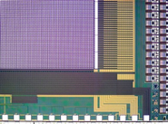
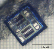
Figure 1 Smart docking chip. L: CMOS3 dock (like CMOS2) with 65536 13x13µm electrodes arranged in 128x128 2x2 electrode pixels containing both actors and sensors and an active area of 4.6x4.6 mm. R. Detail of one corner of the dock. Top left begins the array, which is framed by larger electrodes to control the solution potential. Below are bonding pads to link the chip with an external control board.
The second generation of the dock (DOCK2) provides a more regular and higher density array (128x128) of simpler pixels, each intended to support an elementary actuator and sensing function with just four microelectrodes (2 connected as an actuator, 2 for a sensor with reference). Each electrode has an area of 12x12µm, the whole pixel is 36x36µm large. Overall, approximately 16000 pixels cover an area of 4,6x4, 6mm.
Lablet docking is still supported on any 3x3 pixel square, increasing the number of sites for docking control. Sensors are designed to be activatable without loss in sensitivity, in order to allow run-time coating/recoating electrochemically.
The third generation of the dock is a redesign of the second generation docking station DOCK2, but has implemented a novel sensitive circuitry to allow for electrochemical coating of individual sensors at runtime. Furthermore, the electrodes are enlarged to an area of 13x13µm.
The computer control of the docking chip required the development of two printed circuit boards (for each generation): a docking chip carrier (in microscope slide format) and a USB computer interface FPGA controller board, see fig. 2. The FPGA allowed reconfigurable control of both the CMOS2 and 3 docks with the same board and successive interface improvements to be passed on to partners remotely.
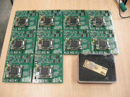
Figure 2 Miniseries of interface electronics and docking PCB.
The FPGA contains a microcontroller that allows programmable control in assembler in addition to special digital circuits controlling the clocks, ADC, DAC and other chips that interface with the flex-cable connecting to the dock carrier. On the host side, a library of communication routines written in C perform the low level control of the FPGA which contains a virtual image of the pixel configuration of the dock. Each pixel on the dock can be individually configured in one of 16 different ways for reading and/or writing of actors and sensors and also individually linked up to one of 8 programmable voltage sources in the range of 0 to 3.3V. The solution potential is set to an intermediate value using large counter electrodes (either collections of pixels, or dedicated large electrodes at the chip periphery) allowing both positive and negative voltage potentiostat operation using either pseudo reference electrodes from pixels in read mode or a true micropipette reference electrode (e.g. Ag/AgCl) which can be connected to a high impedance input on the board. Pixel based current measurements are also possible. The entire array can be updated at 50 Hz and a sequencer has been programmed into the FPGA to allow faster programmable sequential control of smaller groups of pixels up to a MHz in frequency.

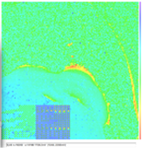
Figure 3. Software interface (mica) for MICREAgents dock control. L Block structure. R. One of the 4 image control panels for the dock pixel array, displaying set pixel voltages in lower left and the electrical image (potentials) of a large fluid droplet (lower left quarter).
A large component in the project involved the multi-tiered software development to connect the docking chip with a user programming environment including graphical user interface and scripting language. The structure of the software is shown in fig. 3. The final version has a python top level interface, ideal for scientist’s extensions and experimental use. RUBc designed the docking chip using a basic pixel unit and programmed modular proliferation of the pixels and connection with bus structures. RUBa made the specification for the docking chip, designed the interface boards, FPGA logic and wrote the entire software hierarchy with an extensive documentation.