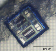

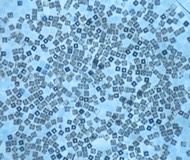
A further highlight of year two and three was the development of a second generation of programmable lablets with full actor and sensor functionality. Fabrication shifted from the simple Europractice multi project wafer to full custom wafer fabrication, using low power transistor design, integrated multilayer galvanic connections, optimised custom slow clocks, optical bar codes, laterally integrated supercaps, and many other features including integrated sensing. A key enabling feature of the 2nd generation CMOS lablets is their modular combinatorial design, separating digital logic variants from interface structures and allowing automated construction of very large combinatorial arrays of lablets for variant testing and experimentation. The new lablets were fabricated and made available for chemical experimentation and in much larger quantities than previously.
Not only lablets but also lablet array chips for testing were fabricated. More details will be available in upcoming publications.
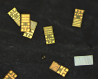
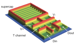
Fig. 1 CMOS2 lablets : Right: layout with simulated 3D profile. Left: examples of singulated CMOS2 lablets, still shown to be electronically functional : 100x200x50µm.