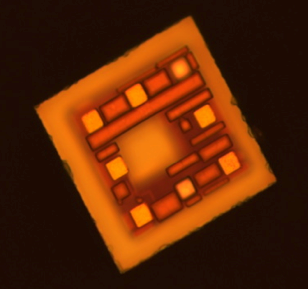
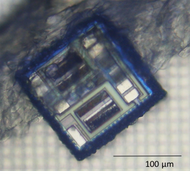
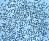
Thousands of 100x100x40µm CMOS lablets designed and produced in year one (without supercaps) were post-processed to change topography, re-metalized with gold coated electrodes, and thinned, diced, and distributed to partners for testing at the beginning of year two. Partners also received non-CMOS test structures with laminates on gold and electrode-structured nickel substrates as mock lablets (designed to emulate supercap integrated lablets) to test chemistry and physical label processing. Dock integrated lablets were tested directly, revealing correct electronic functionality. Electrical connections and current passing through non-connected lablets were successfully demonstrated by a novel use of bipolar electrochemistry via electrochemiluminescence (using a Ru2+ complex). External electrical fields (ca. 15 V/mm) applied in a specially constructed macroscopic lablet test reactor proved sufficient to demonstrate specific optical responses on lablet electrodes. In addition to this test verification, this process indicates that external electric fields can also be used as a source of power for lablets, utilising bipolar Faradaic reactions.

Figure 1: CMOS first generation lablet designed by RUBa,c: dimensions 100x100x40 µm. The 8 equal-sized lighter colored squares are gold-coated micro electrodes exposed to the solution. The other structures are insulated filler or capacitor structures. Specific corner electrodes light up via bipolar ECL proving electrical CMOS wiring as planned (see text).
Lablet development in year two included extensive work on the supercapacitor and power component for the autonomous operation. This work was separately but compatibly investigated, to the main lablet design, using a probe card wafer run and evaluated in WP5 - see text there. In addition other test structures e.g. for sensors were produced.


