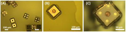

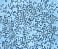
In year one, we completed both a first thinned CMOS chip for lablets and several rounds of non-CMOS lablets all in the 100x100µm size range, and thicknesses varying between 20 and 40µm.
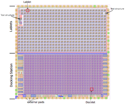
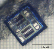
Lablets and docklets, CMOS layout. The overall dimensions of the chip are 5x5 mm.
CMOS chip for lablets and dock (5mm)
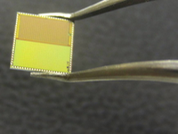
The design of the CMOS chip was focussed primarily on testing the core lablet and docket functionality, and the 5x5 mm chip was divided into two equal parts with arrays of lablets and dockets. The CMOS chips were fabricated (via Europractice, TMSC) and then thinned (Disco).
A separate thin film layer structured with lablets supporting both electrodes and an interdigital supercapacitor structure was designed by RUB and fabricated at Temicon GmbH, together with other simpler test lablet structures, such as those shown below. These lablets are multilayer laminates which support both metal and insulator parts and have densities less than three times water to allow magnetic levitation. The more complex functional lablet designs will be published by RUB in the near future. In addition post-fabrication processing on reassembled wafers, based on the active CMOS chips is currently underway in collaboration with several cleanroom facilities. A complete wafer-level process flow has been developed to allow planarized lablets with gold electrodes and microstructures reactors starting from individual thinned CMOS chips.