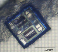


In this work package, the lablets are being designed and fabricated. Design and fabrication separate into two major parts: thinned CMOS electronics and the functional electrochemical microreactor layer. In more detail, fabrication requires a combination of CMOS electronics design, CMOS fab, thinning, reassembly, design and fab post processing for microstructures electrodes, super cap and functionality, separation processing. These functionalities can in part be designed and tested separately and integrated.
This WP does not include the final solution stages of lablet chemical processing as addressed in WP 1-4. The components developed separately in WP 5 (in particular the supercaps and other non-standard or optimized low-power circuit elements) will be integrated. The docking station design and fabrication in WP 7 will reuse the design and fab developments in this WP, involving docklets of the same size as lablets, but differ in the power supply and programmable connections to an external computer. The major steps involved in the is WP are:
1) Complete high level design specification of overall lablet functionality
2) Circuit design, test and optimization for lablet electronics
3) CMOS circuit production on MPWs compatible with post-processing, 2D or 3D)
4) Chip re-assembly for parallel post-processing and lablet testing
5) Post-processing of lablets for electrodes, microreactors and if not in 3 TSVs
6) Supercap integration in lablets with optional coating for photo-power
7) Lablet chemical functionalization and release
8) Verification of lablet programming and functionality via docking stating